
How Google’s Tensor Processing Unit (TPU) Works?

4 Key Insights for Scaling LLM Applications (Sponsored)

LLM workflows can be complex, opaque, and difficult to secure. Get the latest ebook from Datadog for practical strategies to monitor, troubleshoot, and protect your LLM applications in production. You’ll get key insights into how to overcome the challenges of deploying LLMs securely and at scale, from debugging multi-step workflows to detecting prompt injection attacks.
Disclaimer: The details in this post have been derived from the details shared online by the Google Engineering Team. All credit for the technical details goes to the Google Engineering Team. The links to the original articles and sources are present in the references section at the end of the post. We’ve attempted to analyze the details and provide our input about them. If you find any inaccuracies or omissions, please leave a comment, and we will do our best to fix them
When DeepMind’s AlphaGo defeated Go world champion Lee Sedol in March 2016, the world witnessed a big moment in artificial intelligence. The match was powered by hardware Google had been running in production for over a year, but had never publicly acknowledged.
The Tensor Processing Unit, or TPU, represented something more profound than just another fast chip. It marked a fundamental shift in computing philosophy: sometimes doing less means achieving more.
Ever since then, Google’s TPU family has evolved through seven generations since 2015, scaling from single-chip processing image recognition queries to 9216-chip supercomputers training the largest language models in existence. In this article, we look at why Google built custom silicon, and how it works, revealing the physical constraints and engineering trade-offs they had to make.
The Need for TPU
In 2013, Google’s infrastructure team ran a calculation. If Android users adopted voice search at the scale Google anticipated, using it for just three minutes per day, the computational demand would require doubling the company’s entire global data center footprint.
This was a problem with no obvious solution at the time. Building more data centers filled with traditional processors was economically unfeasible. More critically, Moore’s Law has been slowing for years. For decades, the semiconductor industry had relied on the observation that transistor density doubles roughly every two years, delivering regular performance improvements without architectural changes. However, by 2013, this trend was weakening. Google couldn’t simply wait for Intel’s next generation of CPUs to solve its problem.
The root cause of this situation was architectural. Traditional computers follow the Von Neumann architecture, where a processor and memory communicate through a shared bus. To perform any calculation, the CPU must fetch an instruction, retrieve data from memory, execute the operation, and write results back. This constant transfer of information between the processor and memory creates what computer scientists call the Von Neumann bottleneck.
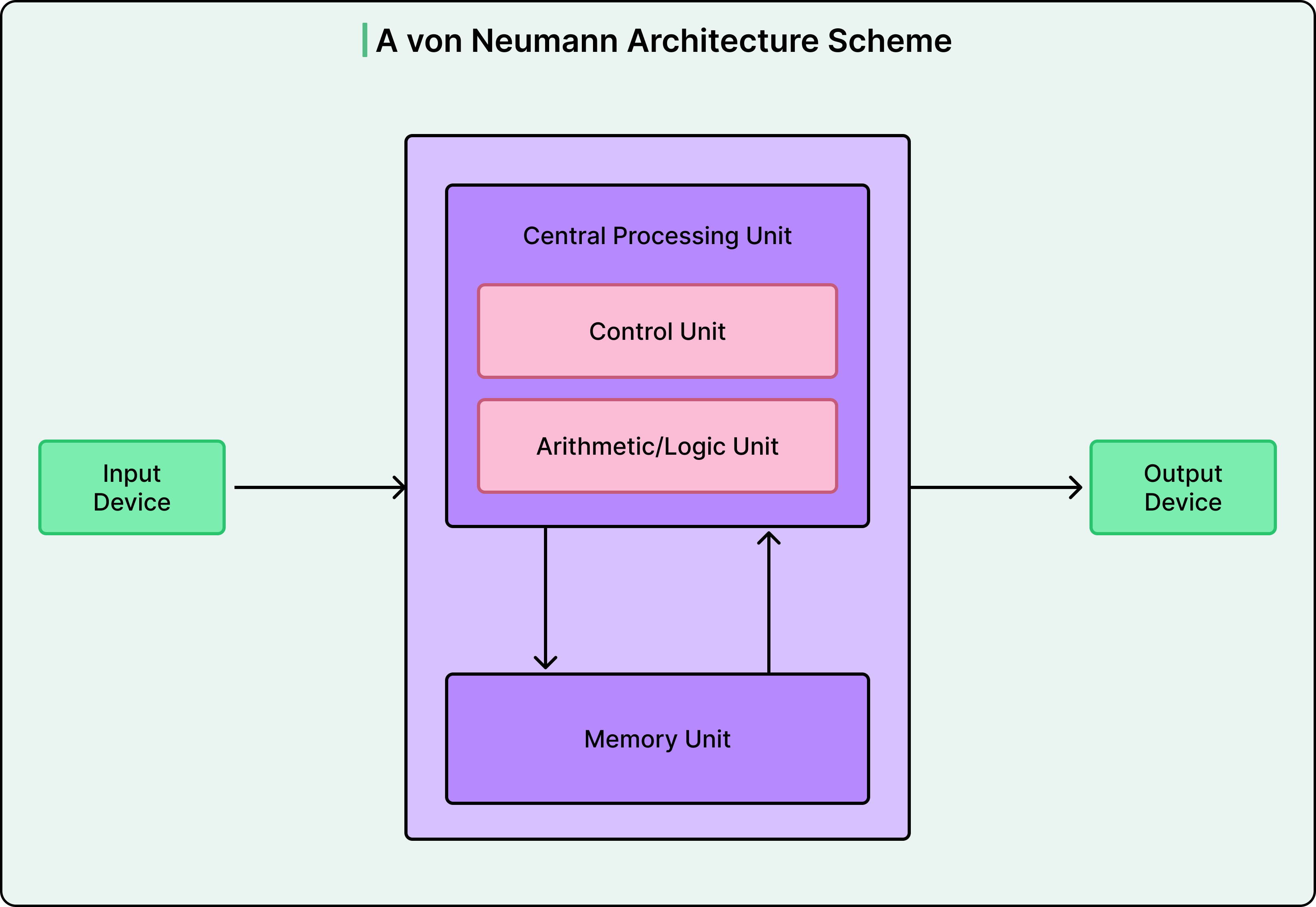
The energy cost of moving data across this bus often exceeds the energy cost of the computation itself. For example, imagine a chef preparing a meal but having to walk to a distant pantry for each ingredient. The cooking takes seconds, but the walking consumes hours. For general-purpose computing tasks like word processing or web browsing, this design makes sense because workloads are unpredictable. However, neural networks are different.
Deep learning models perform one operation overwhelmingly: matrix multiplication. A neural network processes information by multiplying input data by learned weight matrices, adding bias values, and applying activation functions. This happens billions of times for a single prediction. Modern language models with hundreds of billions of parameters require hundreds of billions of multiply-add operations per query. Critically, these operations are predictable, parallel, and deterministic.
CPUs devote significant processing power to features like branch prediction and out-of-order execution, designed to handle unpredictable code. Graphics Processing Units, or GPUs, improved matters with thousands of cores working in parallel, but they still carried architectural overhead from their graphics heritage. Google’s insight was to build silicon that does only what neural networks need and strip away everything else.
The Systolic Array: A Different Way to Compute
The heart of the TPU is an architecture called a systolic array. The name originates from the Greek word for heartbeat, referencing how data pulses rhythmically through the chip. To understand why this matters, consider how different processors approach the same task.
A CPU operates like a single worker running back and forth between a water well and a fire, filling one bucket at a time.
A GPU deploys thousands of workers making the same trips simultaneously. Throughput increases, but the traffic between the well and the fire becomes chaotic and energy-intensive.
A systolic array takes a fundamentally different approach. The workers form a line and pass buckets hand to hand. Water flows through the chain without anyone returning to the source until the job is complete.
In a TPU, the workers are simple multiply-accumulate units arranged in a dense grid. The first-generation TPU used a 256 by 256 array, meaning 65,536 calculators operating simultaneously. Here’s how computation proceeds:
Neural network weights are loaded into each calculator from above and remain stationary.
Input data flows in from the left, one row at a time.
As data passes through each calculator, it is multiplied by the resident weight.
The product adds to a running sum, then passes rightward to the next calculator.
Partial results accumulate and flow downward.
Final results emerge from the bottom after all calculations are complete.
See the diagram below:
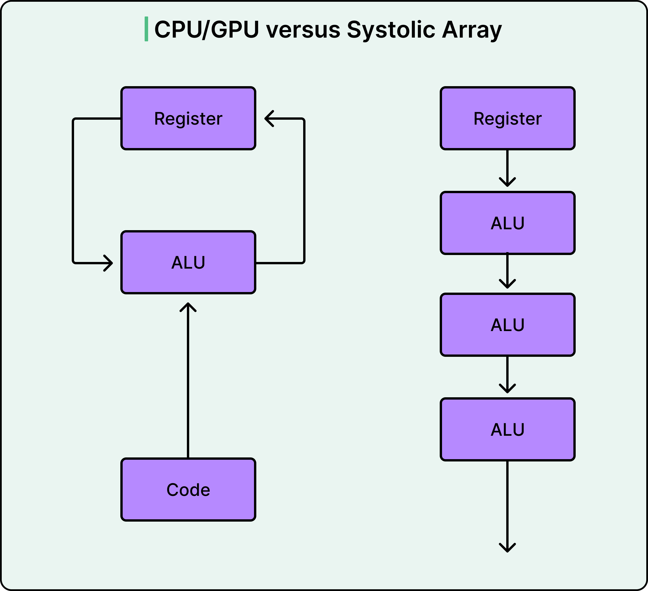
This design means data is read from memory once but used thousands of times as it traverses the array. Traditional processors must access memory for nearly every operation. The systolic array eliminates this bottleneck. Data moves only between spatially adjacent calculators over short wires, dramatically reducing energy consumption.
The numbers make a strong case for this approach.
TPU v1’s 256 by 256 array could perform 65536 multiply-accumulate operations per clock cycle. Running at 700 MHz, this delivered 92 trillion 8-bit operations per second while consuming just 40 watts.
A contemporary GPU might perform tens of thousands of operations per cycle, while the TPU performed hundreds of thousands.
More than 90 percent of the silicon performed useful computation, compared to roughly 30 percent in a GPU.
The trade-off here is absolute specialization. A systolic array can only perform matrix multiplications efficiently. It cannot render graphics, browse the web, or run a spreadsheet. Google accepted this limitation because neural network inference is fundamentally matrix multiplication repeated many times.
The Supporting Architecture
The systolic array requires carefully orchestrated support components to achieve its performance. Each piece solves a specific bottleneck in the pipeline from raw data to AI predictions.
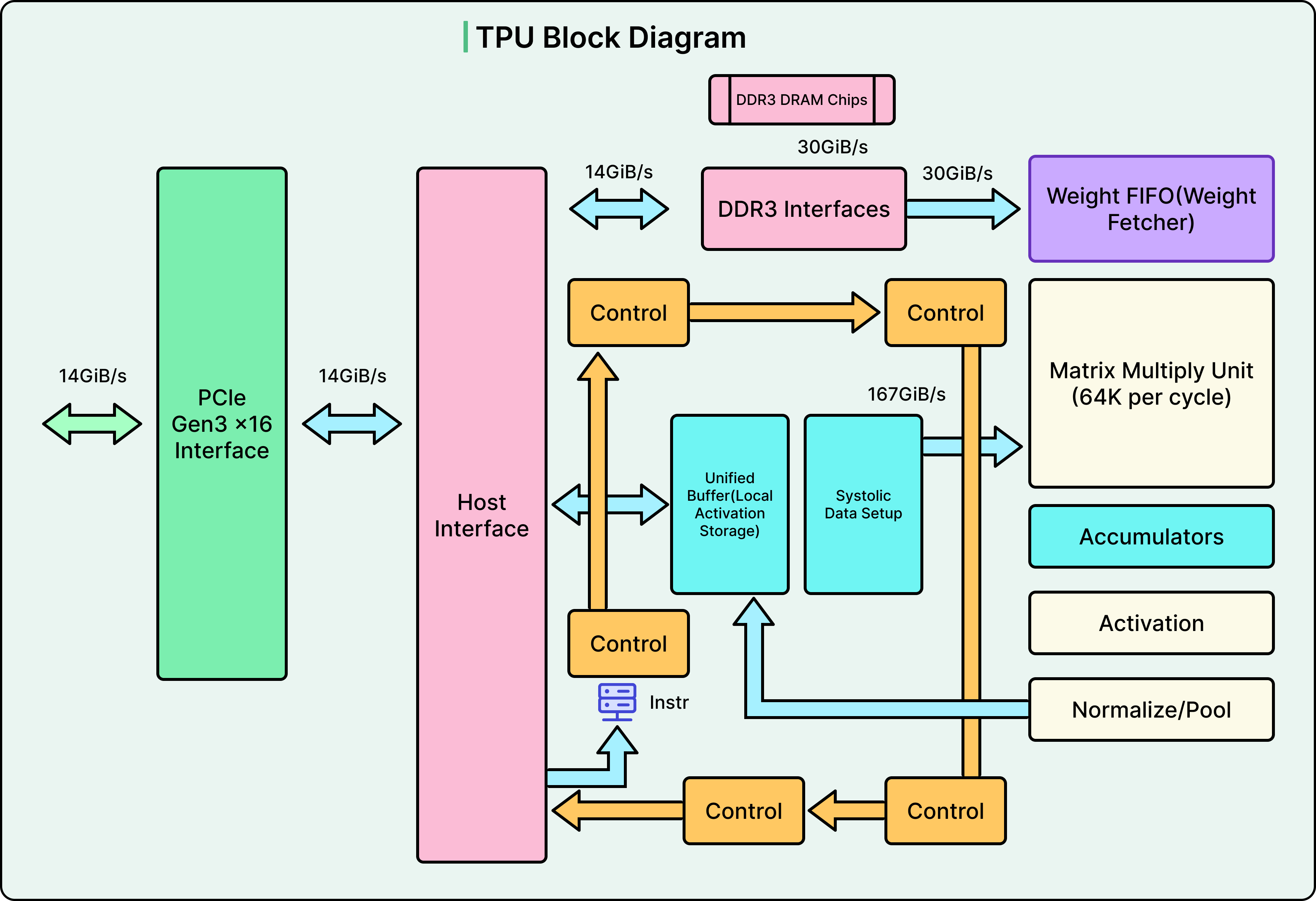
Let’s look at the most important components:
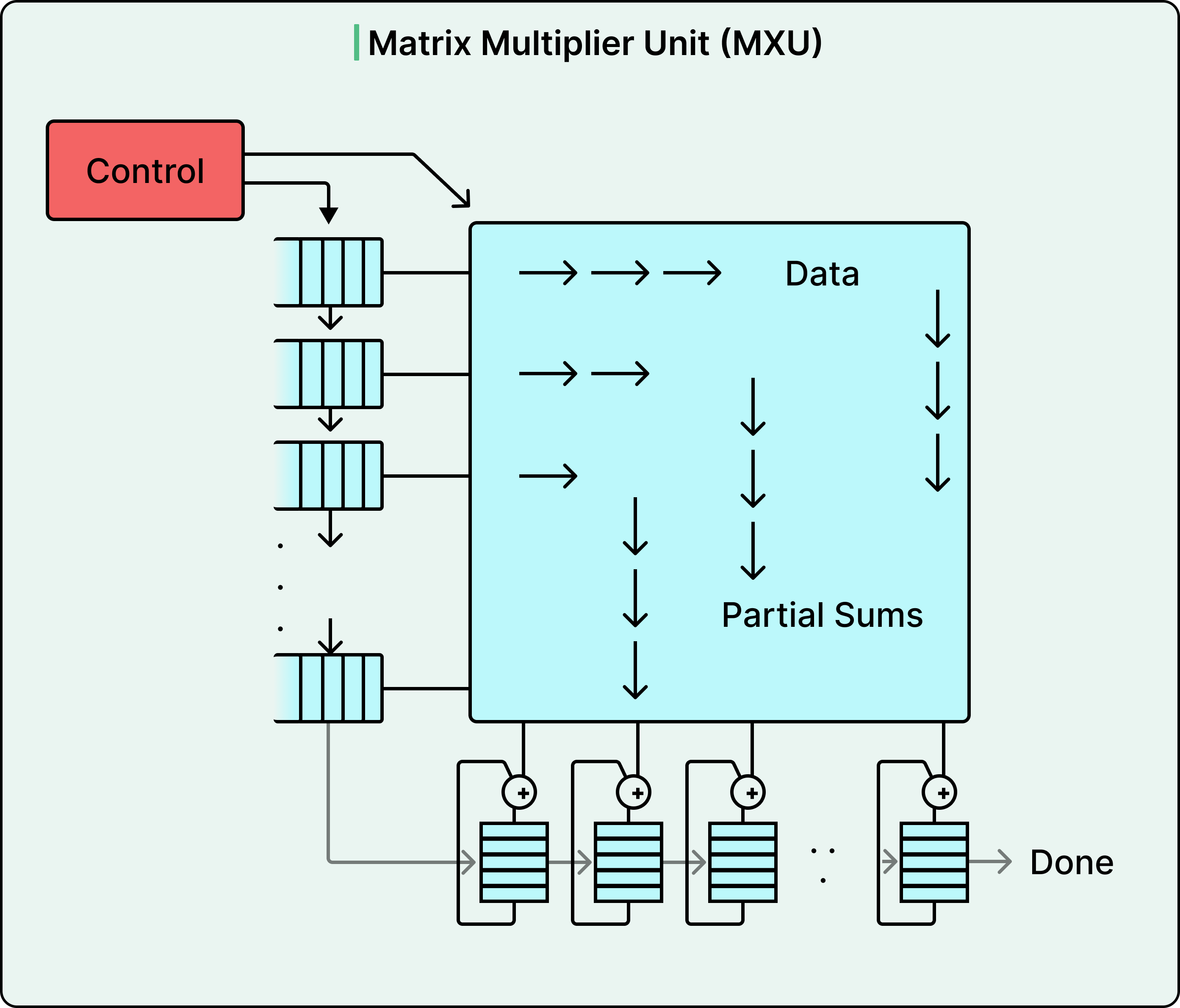
The Matrix Multiply Unit
The Matrix Multiply Unit, or MXU, is the systolic array itself.
TPU v1 used a single 256-by-256 array operating on 8-bit integers. Later versions shifted to 128 by 128 arrays using Google’s BFloat16 format for training workloads, then returned to 256 by 256 arrays in v6 for quadrupled throughput. The weight-stationary design minimizes data movement, which is the primary consumer of energy in computing.
Unified Buffer
The Unified Buffer provides 24 megabytes of on-chip SRAM, serving as a high-speed staging area between slow external memory and the hungry MXU.
This buffer stores input activations arriving from the host computer, intermediate results between neural network layers, and final outputs before transmission. Since this memory sits directly on the chip, it operates at a higher bandwidth than external memory. This difference is critical for keeping the MXU continuously fed with data rather than sitting idle waiting for memory access.
Vector Processing Unit
The Vector Processing Unit handles operations that the MXU cannot. This includes activation functions like ReLU, sigmoid, and tanh.
Neural networks require non-linearity to learn complex patterns. Without it, multiple layers would collapse mathematically into a single linear transformation. Rather than implementing these functions in software, the TPU has dedicated hardware circuits that compute activations in a single cycle. Data typically flows from the MXU to the VPU for activation processing before moving to the next layer.
Accumulators
Accumulators collect the 32-bit results flowing from the MXU.
When multiplying 8-bit inputs, products are 16-bit, but accumulated sums grow larger through repeated addition. Using 32-bit accumulators prevents overflow during the many additions a matrix multiplication requires. The accumulator memory totals 4 megabytes across 4,096 vectors of 256 elements each.
Weight FIFO Buffer
The Weight FIFO buffer stages weights between external memory and the MXU using a technique called double-buffering.
The MXU holds two sets of weight tiles: one actively computing while the other loads from memory. This overlap completely hides memory latency, ensuring the computational units never wait for data.
High Bandwidth Memory
High Bandwidth Memory evolved across TPU generations.
The original v1 used DDR3 memory delivering 34 gigabytes per second. Modern Ironwood TPUs achieve 7.4 terabytes per second, a 217-fold improvement. HBM accomplishes this by stacking multiple DRAM dies vertically with thousands of connections between them, enabling bandwidth impossible with traditional memory packaging.
The Precision Advantage
TPUs gain significant efficiency through quantization, using lower-precision numbers than traditional floating-point arithmetic. This choice has big hardware implications that cascade through the entire design.
Scientific computing typically demands high precision. Calculating pi to ten decimal places requires careful representation of very small differences. However, neural networks operate differently. They compute probabilities and patterns. For example, whether a model predicts an image is 85 percent likely to be a cat versus 85.3472 percent likely makes no practical difference to the classification.
A multiplier circuit’s silicon area scales with the square of the bit width. An 8-bit multiplier requires roughly 64 units of silicon area, whereas a 32-bit multiplier requires about 576 units. This mathematical relationship explains why TPU v1 could pack 65,536 multiply-accumulate units into a modest chip while a GPU contains far fewer floating-point units. More multipliers mean more parallel operations per cycle.
The first TPU used 8-bit integers for inference, reducing memory requirements by four times compared to 32-bit floats. A 91-megabyte model becomes 23 megabytes when quantized. Research demonstrated that inference rarely needs 32-bit precision. The extra decimal places don’t meaningfully affect predictions.
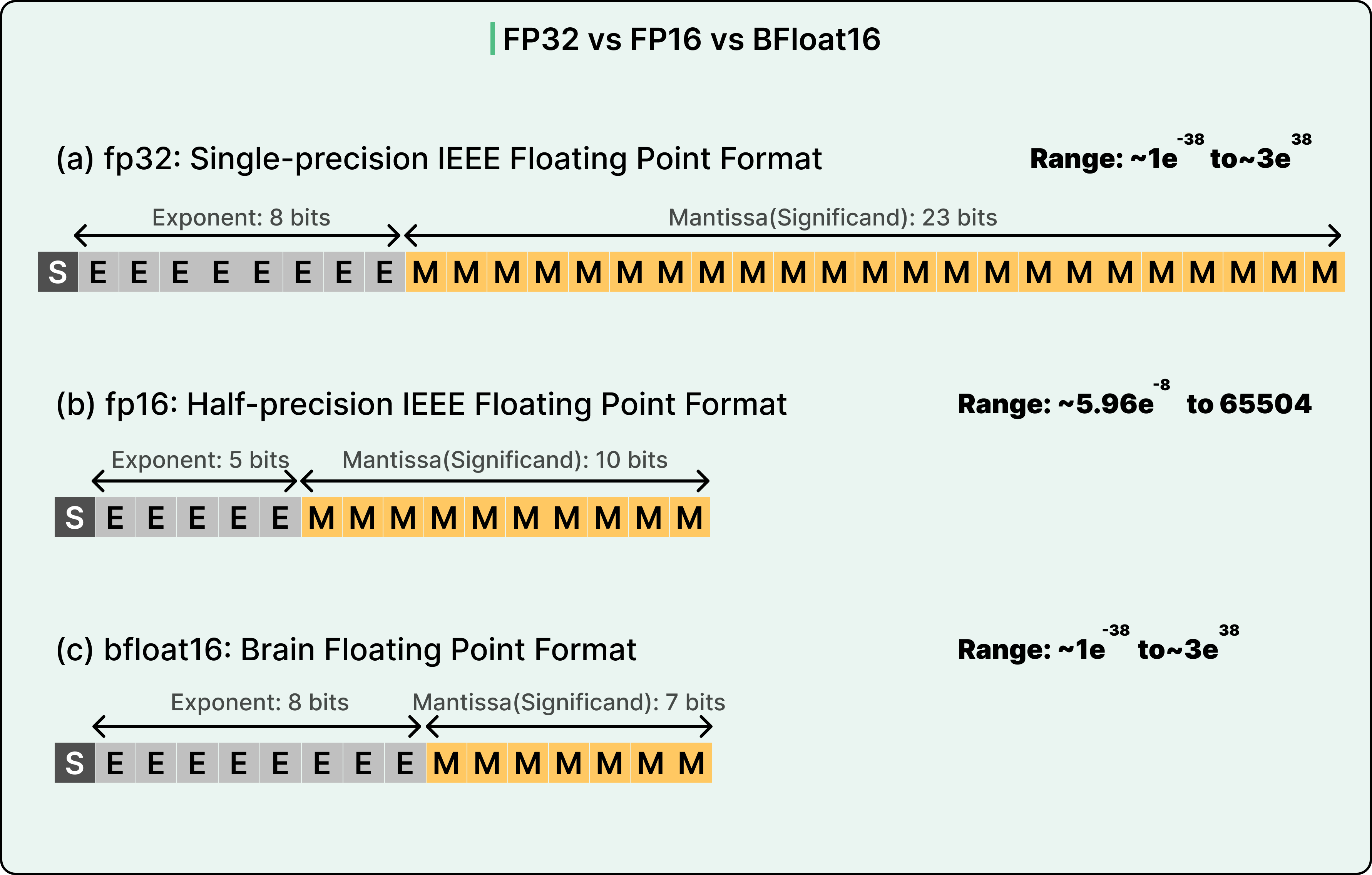
Training requires more precision because small gradient updates accumulate over millions of iterations. Google addressed this by inventing BFloat16, or Brain Floating-Point 16. This format maintains the same 8-bit exponent as a 32-bit float but uses only 7 bits for the mantissa. The key insight was that neural networks are far more sensitive to dynamic range, controlled by the exponent, than to precision, controlled by the mantissa. BFloat16 provides a wide range of floating-point formats with half the bits, enabling efficient training without the overflow problems that plagued alternative 16-bit formats.
See the diagram below:
Modern TPUs support multiple precision modes.
BFloat16 for training.
INT8 for inference runs twice as fast on TPU v5e,
The newest FP8 format.
Ironwood is the first TPU with native FP8 support, avoiding the emulation overhead of earlier generations.
Evolution Journey
TPU development follows a clear trajectory.
Each generation increased performance while improving energy efficiency. The evolution reveals how AI hardware requirements shifted as models scaled.
TPU v1 launched secretly in 2015, focusing exclusively on inference. Built on 28-nanometer process technology and consuming just 40 watts, it delivered 92 trillion 8-bit operations per second. The chip connected via PCIe to standard servers and began powering Google Search, Photos, Translate, and YouTube before anyone outside Google knew it existed. In March 2016, TPU v1 powered AlphaGo’s victory over Lee Sedol, proving that application-specific chips could beat general-purpose GPUs by factors of 15 to 30 times in speed and 30 to 80 times in power efficiency.
TPU v2 arrived in 2017 with fundamental architecture changes to support training. Replacing the 256 by 256 8-bit array with two 128 by 128 BFloat16 arrays enabled the floating-point precision training requires. Adding High Bandwidth Memory, 16 gigabytes at 600 gigabytes per second, eliminated the memory bottleneck that limited v1. Most importantly, v2 introduced the Inter-Chip Interconnect, custom high-speed links connecting TPUs directly to each other. This enabled TPU Pods where 256 chips operate as a single accelerator delivering 11.5 petaflops.
TPU v3 in 2018 doubled performance to 420 teraflops per chip and introduced liquid cooling to handle increased power density. Pod size expanded to 1,024 chips, exceeding 100 petaflops, enough to train the largest AI models of that era in reasonable timeframes.
TPU v4 in 2021 brought multiple innovations. SparseCores accelerated embedding operations critical for recommendation systems and language models by five to seven times using only 5 percent of the chip area. Optical Circuit Switches enabled dynamic network topology reconfiguration. Instead of fixed electrical cables, robotic mirrors steer beams of light between fibers. This allows the interconnect to route around failures and scale to 4,096-chip Pods approaching one exaflop. The 3D torus topology, with each chip connected to six neighbors instead of four, reduced communication latency for distributed training.
Ironwood, or TPU v7, launched in 2025 and represents the most significant leap. Designed specifically for the age of inference, where deploying AI at scale matters more than training, each chip delivers 4,614 teraflops with 192 gigabytes of HBM at 7.4 terabytes per second bandwidth.
Conclusion
TPU deployments demonstrate practical impact across diverse applications.
For reference, a single TPU processes over 100 million Google Photos per day. AlphaFold’s solution to the 50-year protein folding problem, earning the 2024 Nobel Prize in Chemistry, ran on TPUs. Training PaLM, a 540-billion-parameter language model, across 6,144 TPU v4 chips achieved 57.8 percent hardware utilization over 50 days, remarkable efficiency for distributed training at that scale. Beyond Google, TPUs power Anthropic’s Claude assistant, Midjourney’s image generation models, and numerous research breakthroughs.
However, TPUs aren’t universally superior. They excel at large-scale language model training and inference, CNNs and Transformers with heavy matrix operations, high-throughput batch processing, and workloads prioritizing energy efficiency. On the other hand, GPUs remain better choices for PyTorch-native development, which requires the PyTorch/XLA bridge with some friction. Small batch sizes, mixed AI and graphics workloads, multi-cloud deployments, and rapid prototyping often favor GPUs.
TPUs represent a broader industry shift toward domain-specific accelerators.
The general-purpose computing model, where CPUs run any program reasonably well, hits physical limits when workloads scale to trillions of operations per query. Purpose-built silicon that sacrifices flexibility for efficiency delivers order-of-magnitude improvements that no amount of general-purpose processor optimization can match.
References:
SPONSOR US
Get your product in front of more than 1,000,000 tech professionals.
Our newsletter puts your products and services directly in front of an audience that matters - hundreds of thousands of engineering leaders and senior engineers - who have influence over significant tech decisions and big purchases.
Space Fills Up Fast - Reserve Today
Ad spots typically sell out about 4 weeks in advance. To ensure your ad reaches this influential audience, reserve your space now by emailing sponsorship@bytebytego.com.
I had no interest in this topic but once I started reading through I couldn't stop. What an fantastic way to explain complex concept! Truly one of the best newsletter I subscribe to.
Jax seems the only native option to operate tpus but it’s still less mature than PyTorch. I wish PyTorch can merge xla as one of its backend.